Map losses within solar cells
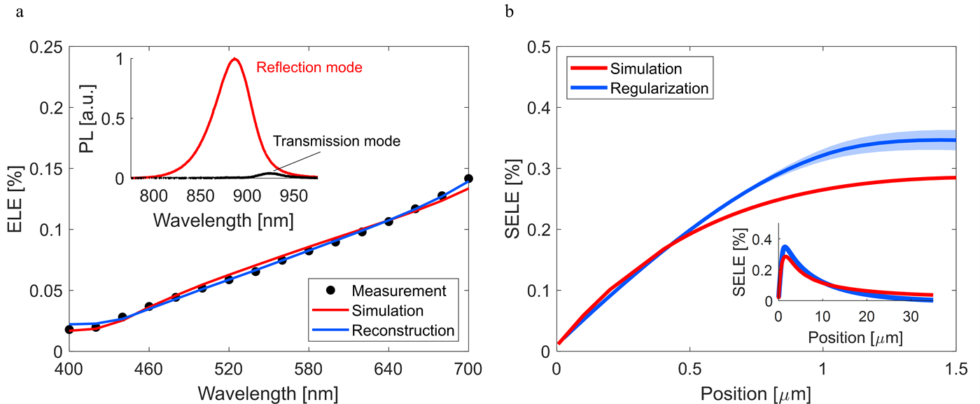
My research focused on developing a new method for mapping losses within solar cells. We did this by combining custom photoluminescence (PL) measurement setups, optical modeling, semiconductor physics, and simulations in COMSOL Multiphysics. This method uses different illumination wavelengths to probe into different depths in the material, and can be used in manufecturing process or in post processing tools for semiconductor devices.
Published in ACS Applied Energy Materials
This extensive work was published in ACS Applied Energy Materials in 2024. The main text describes the method, developed using PL measurements on GaAs wafers and optical modeling. The text describe the mathematical reasoning behind the SELE extraction, and the simulation in COMSOL that were used to validate the experimental results. This publish also included a new photon-recycling model. The supplementary information is very extensive and covers detailed information about the method and validation process.
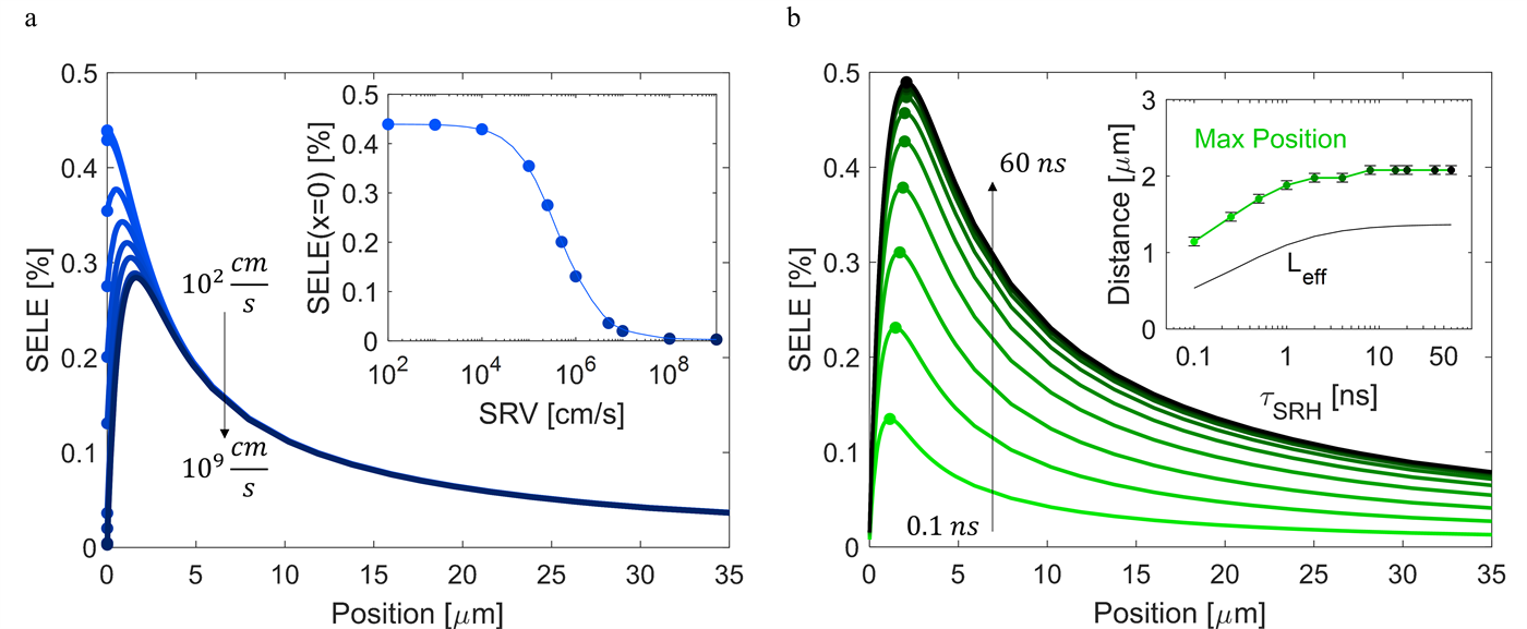
The research page interactive research graphs shows the SELE profiles with applicative sliders, that allows you to explore the different PL and SELE profiles for different excitation wavelength, surface recombination velocity, and carrier lifetime.
Photon recycling using ray optics
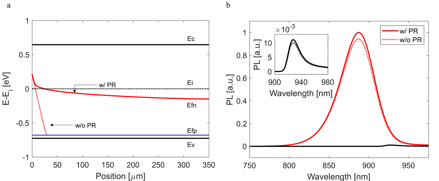
The photon recycling model connects the optical picture to the semiconductor physics. Photons emitted by radiative recombination are not simply lost: some are reabsorbed deeper in the device, creating new carriers and reshaping the measured luminescence profile. Modeling that process helped separate surface losses from bulk transport effects and was crucial for extracting accurate SELE profiles.
Read more in our paper here.
Read the paper on ACS