Mapping losses through empirical extraction of the Spatial External Luminescence Efficiency
Tel Aviv University, Energy Devices Lab, supervised by Dr. Gideon Segev.
Solar cells lose efficiency not only because of the material they are made from, but because of where charge carriers are lost inside the device: at surfaces, interfaces, depletion regions and in the bulk. My PhD developed a way to map those losses in depth using photoluminescence measurements and optical modeling.
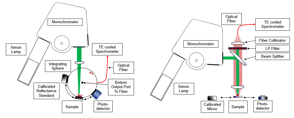
The method extracts a Spatial External Luminescence Efficiency (SELE) profile: the probability that an electron-hole pair generated at a specific depth will eventually contribute to the emitted photoluminescence. In practice, that turns wavelength-dependent PL into a depth-resolved view of recombination, transport and voltage loss.
Extract SELE from PL
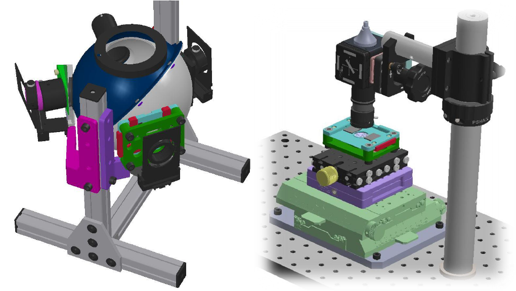
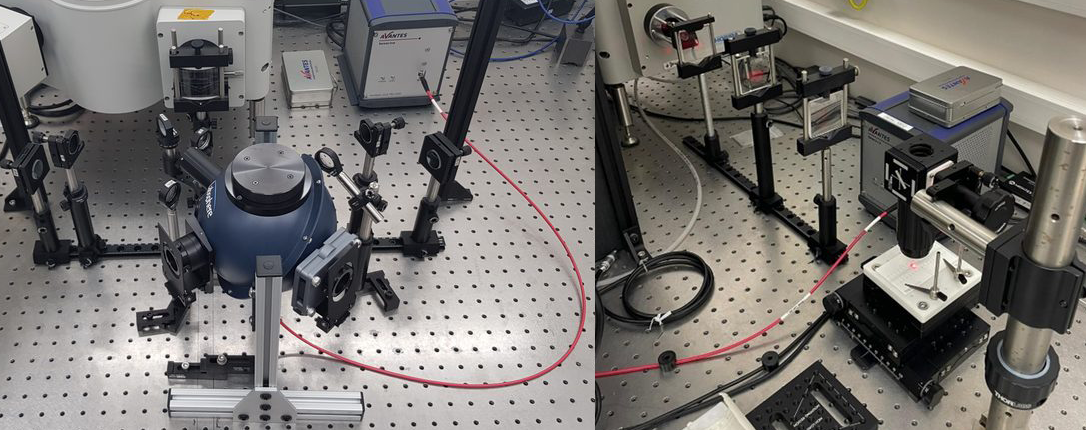
Built the inverse method using wavelength-dependent PL, transfer-matrix optical generation profiles and regularization tools.
Validate the physics
Compared measured GaAs profiles with COMSOL drift-diffusion simulations and a photon-recycling model.
Map devices
Applied SELE to PN junctions and PV-cell structures, including the effect of the space-charge region on emitted PL.
Probe surfaces
Used MOS capacitors and dynamic native-oxide formation measurements to study surface and interface behavior.
SELE of GaAs, PL measurements and SELE simulations
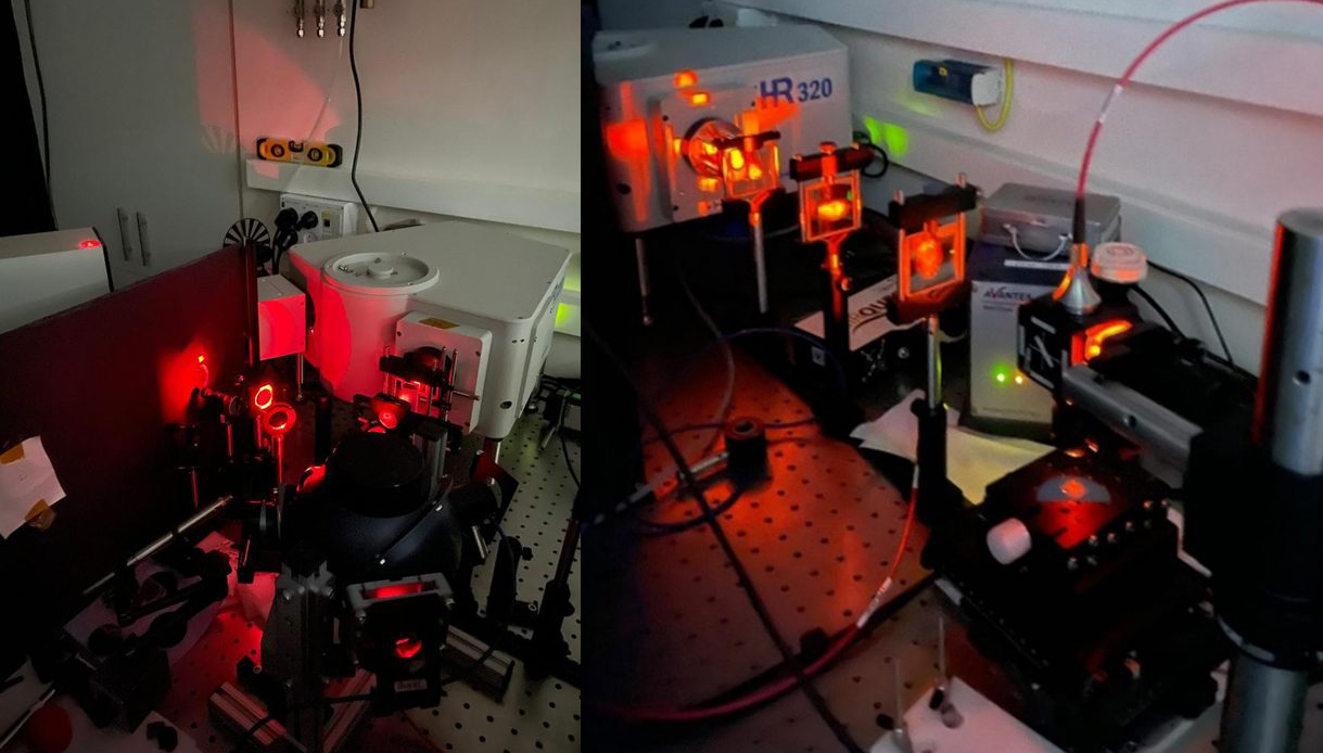
These interactive figures show the core idea behind the method. Different excitation wavelengths are absorbed at different depths in GaAs, so sweeping the excitation wavelength probes different regions of the sample. The extracted SELE profiles then connect the measured PL response to surface recombination, bulk lifetime and diffusion length.
Simulated SELE profiles of p-type GaAs wafers. Left: SELE profiles for wafers with surface recombination velocity between 102 cm/s and 109 cm/s and τSRH of 0.6 ns. Right: simulated SELE profiles for wafers with τSRH between 0.1 ns and 60 ns and a surface recombination velocity of 4 · 107 cm/s. All values correspond to the parameters of the minority carriers in simulation.
What the method made visible
- Surface recombination velocity changes the SELE profile close to the illuminated surface.
- Bulk lifetime and diffusion length shift the shape and peak position of the depth profile.
- SELE can estimate voltage loss and possible voltage gain from better passivation.
- In PN junctions, the profile can reveal where charge carriers are swept by the space-charge region.
- Dynamic PL measurements can track surface processes such as native oxide formation on GaAs.